The canonical "hello world" program for microcontrollers is commonly known as
Blink. The program takes many forms, but generally amounts to this:
6.1.2. Blink
- Turn on an LED.
- Wait a second or so.
- Turn off the LED.
- Go to step 1.
We're going write an increasingly difficult version of Blink, referencing the datasheets for all necessary
information. The first version will be written in
AVR assembler
(but assembled using the free
GCC
compiler), and we'll proceed to the C version afterwards. Assembly language examples are written using the
GNU Assembler.
The AVR architecture used in the ATMega328p is slightly atypical in that it is an unmodified
Harvard architecture
with completely separate address spaces for code and data. C/C++ programmers are, at the time of writing,
accustomed to having code and data live within the same address space. The reason this is important to mention
is because it's often necessary to specify the addresses of functions and objects when programming
microcontrollers, and it's critical to understand that address 0x0000 in program
space is not the same as address 0x0000 in data space! The AVR actually exposes
different instructions to read from and write to locations in program space as opposed to data space. This can
have practical consequences when programming in C on this architecture, because although the ATMega328p has 32
kilobytes of code space, it only has 2 kilobytes of data space. A programmer that declares a variable of type
const unsigned char[2048]
might be dismayed to realize that they've just consumed the entirety of the working memory on the system,
despite the fact that the variable is const and could fit comfortably into the 32
kilobytes of code space. In order for a const variable to be placed into code
space, it's necessary to use Named Address Spaces from the current
N1275 Embedded C
draft standard. Named address spaces are available as a
GCC extension
, and we'll be revisiting them later on. The AVR microcontrollers actually use many different address spaces,
but we'll only be seeing a few of them in this book.
Throughout this document, the following notation will be used:
6.2.3. Address Spaces
- code@0xNNNN denotes address 0xNNNN in code space.
- data@0xNNNN denotes address 0xNNNN in data space.
- io@0xNNNN denotes address 0xNNNN in I/O space.
As soon as the microcontroller powers on, it begins executing code from a location specified by the fuse
bit BOOTRST. The default configuration for the ATMega328p specifies
that BOOTRST = 0, and page 276 of the datasheet indicates that this means that
execution will start at program address code@0x0000 when the microcontroller is
powered on. We won't be changing this default setting.
The code that lives at code@0x0000 represents the
interrupt table. The interrupt table is a 26-element array where each element consists
of two instruction words. The instructions will, in practice, typically always perform an unconditional jump to
some subroutine in memory.
The full table of interrupts is described on page 74 of the datasheet:
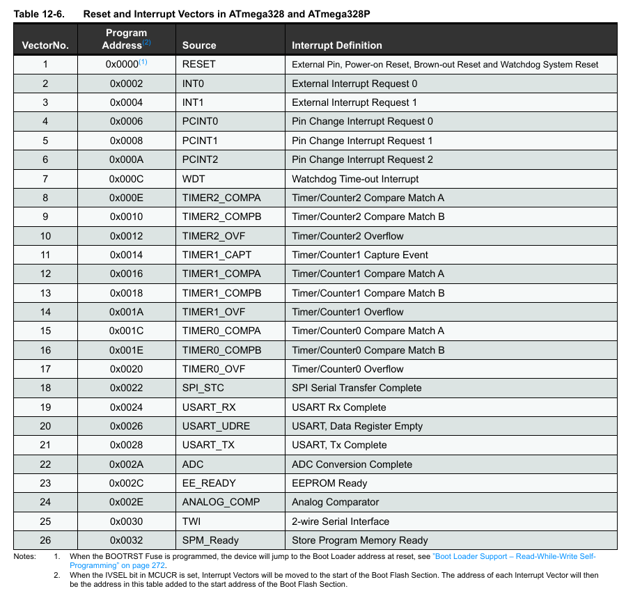
The first element of the interrupt table is executed in response to a RESET interrupt,
and therefore the instructions in this element of the table will always be the first instructions executed when
the microcontroller powers on. Because, in this example, we aren't planning to use interrupts at all, we can
actually provide a very simple interrupt table that simply jumps to a function we provide
called __avr_setup:
6.3.6. AVR Interrupt Table
.text

.global __avr_setup
.global __avr_interrupt_vectors
.global __avr_unexpected_interrupt

.org 0x0000

__avr_interrupt_vectors:
  jmp __avr_setup
  jmp __avr_unexpected_interrupt
  jmp __avr_unexpected_interrupt
  jmp __avr_unexpected_interrupt
  jmp __avr_unexpected_interrupt
  jmp __avr_unexpected_interrupt
  jmp __avr_unexpected_interrupt
  jmp __avr_unexpected_interrupt
  jmp __avr_unexpected_interrupt
  jmp __avr_unexpected_interrupt
  jmp __avr_unexpected_interrupt
  jmp __avr_unexpected_interrupt
  jmp __avr_unexpected_interrupt
  jmp __avr_unexpected_interrupt
  jmp __avr_unexpected_interrupt
  jmp __avr_unexpected_interrupt
  jmp __avr_unexpected_interrupt
  jmp __avr_unexpected_interrupt
  jmp __avr_unexpected_interrupt
  jmp __avr_unexpected_interrupt
  jmp __avr_unexpected_interrupt
  jmp __avr_unexpected_interrupt
  jmp __avr_unexpected_interrupt
  jmp __avr_unexpected_interrupt
  jmp __avr_unexpected_interrupt
  jmp __avr_unexpected_interrupt

__avr_unexpected_interrupt:
  jmp __avr_interrupt_vectors
Essentially, the first entry of the __avr_interrupt_vectors table performs an
unconditional jump to a not-yet-defined function called
__avr_setup. Every other entry in the table first jumps to
__avr_unexpected_interrupt, and then jumps back to the first entry of the
__avr_interrupt_vectors
table. In effect, this causes any interrupt raised to cause the microcontroller to behave as if it had
been reset. The intermediate
__avr_unexpected_interrupt
function purely exists to assist with debugging; the user can set a breakpoint on the
__avr_unexpected_interrupt
function to be notified whenever the program receives an interrupt it wasn't expecting.
Now that interrupts have been configured, and the
execution path of the code leads to the
__avr_setup
function, it's time to actually define that function. The function has three responsibilities:
6.4.2. Setup Actions
- The function must clear the AVR status register.
- The function must set up the AVR stack pointer.
- The function must begin executing the programmer's application code.
The AVR status register (referred to as SREG in the
datasheet) is a register that enables and disables interrupts, and provides information about the most recently
executed arithmetic operation such as indicating overflows, carries, and so on. The status register should be
manually cleared on startup in order to ensure that the microcontroller has a clean slate with regards to
execution state. The status register is accessible at address
io@0x003f, and can be assigned using the special
instruction out, which can store a value in the address range dedicated to the
microcontroller's I/O registers.
The AVR stack pointer points to the top of the execution stack. As with most
architectures, the AVR execution stack grows downwards from higher addresses to lower addresses. The AVR
push
instruction pushes data onto the stack, which results in the stack pointer being decremented by 1. In
other words, if the stack pointer is currently pointing at address data@0x03ff,
and a push instruction is executed, the stack pointer will now be pointing at
address data@0x03fe. The AVR pop instruction is
the exact inverse; the stack pointer will be incremented. It's necessary, on startup of the microcontroller, for
the programmer to initialize the stack pointer to a sensible value. In practice, this value is always the
address of the top of the SRAM. On the ATMega328p, the data sheet indicates on page 28 that the internal SRAM
ranges from
data@0x0100
to data@0x08ff inclusive. The 16-bit stack pointer is implemented as a pair of
8-bit registers, with the high 8 bits at
io@0x003e
and the low 8 bits at
io@0x003d.
Given all of this information, we can now write the __avr_setup function:
6.4.6. AVR Setup
__avr_stack_pointer_h = 0x3e
__avr_stack_pointer_l = 0x3d
__avr_status_register = 0x3f

__avr_setup:
  # Clear the status register
  ldi r16,0x0
  out __avr_status_register,r16

  # Configure the stack pointer to start at 0x08ff
  ldi r16,0x08
  out __avr_stack_pointer_h,r16
  ldi r16,0xff
  out __avr_stack_pointer_l,r16

  # Execute main
  call main
The function loads 0 into register r16, and then
stores the value of r16 into I/O location
0x3f. This clears the status register.
The function then loads 0x08 into register r16, and
stores the value of r16 into I/O location
0x3e. It immediately follows by storing
0xff
into I/O location 0x3d. This has the effect of setting the stack pointer to
0x08ff
- the top of SRAM.
The function then calls a yet-to-be-defined function called main that will
eventually contain our Blink code.
In order to implement Blink, we first need to connect an LED that we can turn on and off from the
microcontroller. On page 13 of the datasheet, we can see numerous
ports
listed that span sets of pins. A port is, essentially, an I/O register: Setting a
single bit in the register to 1 will set the corresponding pin voltage high, whilst
setting the same bit to 0 will set the corresponding pin voltage low. The first
port listed on page 13 is Port B, and we can see that this consists of eight pins/bits named
PB0
to PB7. If we try to find
PB0
on the
pin configuration
diagram on page 12, we'll find that PB0 is associated with pin 14, on the bottom left
corner of the IC. We can see that pin 14 can also be configured to provide a number of different functions, such
as CLKO (the pin used to for the
clock output
we briefly encountered earlier). We can search the datasheet for the definitions of all of these things but, as
we don't need them and they're all disabled by default, it's clear that we can safely use pin 14 to control our
LED.
We can see on page 323 of the datasheet that the minimum output voltage any given ATMega328p will provide on an
output pin when the voltage is set high is 4.2V. The LED specified in the
bill of materials
will be damaged if we supply it with this much current, so we need to connect it in series with a
220Ω
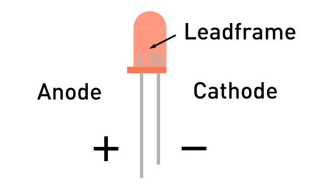
resistor. Note that LEDs are
polarized
components and therefore must be connected in the correct orientation. The
negative
side or cathode of the LED must be connected to ground. LED components always provide
some way to indicate orientation, either by making the positive or
anode
leg of the LED longer, or by angling the internal construction of the internal leadframe
such that it points towards the
positive
side[1]:
6.5.4. Connections
- Connect a 220Ω resistor to pin 14 on the microcontroller.
- Connect an LED to the resistor and to ground.
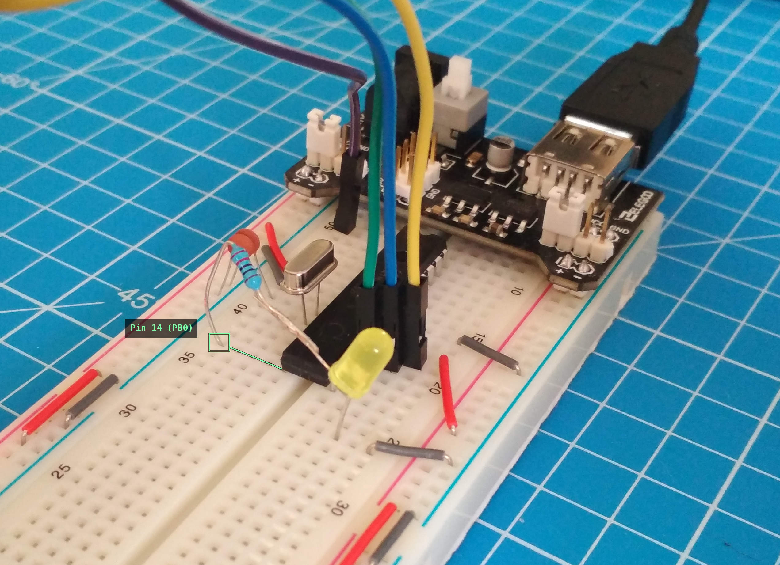
Note that, in the image above, the anode leg of the LED has been soldered to the
resistor rather than both the resistor and the anode leg being plugged into the
breadboard. This is purely for convenience and isn't necessary for the circuit to function.
Now that we have an LED connected, it's time to write the actual function that will turn the LED on and off and
a fixed interval. We know that the LED is connected to Port B, pin
PB0, and page 84 of the datasheet tells us that there are three I/O memory address
locations associated with any given port: A DDR register that controls whether a
pin is used as an input or an output, a PORT register that allows for setting a pin
high or low when the pin is used as an output, and a
PIN
register that is used to read the value of a pin when the pin is used as an input. We can largely ignore the
PIN
register as we're only concerned with output at the moment. The datasheet, over the next few pages,
describes the method to use for reading or writing pins. Reduced to the essentials: We need to set
PB0
as an output pin by setting bit 0 of the DDRB register
to 1, and then we can set the pin high or low by setting bit 0
of the PORTB register to
1
or 0, respectively. We can jump to the complete summary of all registers on the
microcontroller on page 624 to determine the I/O locations of these registers:
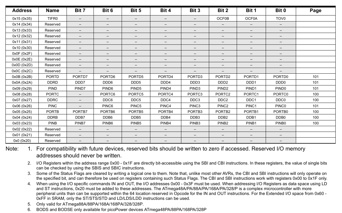
We can see that DDRB is at
io@0x04
and PORTB is at
io@0x05
[2]. All of this amounts to the following assembler
instructions:
6.6.4. Setting LED On/Off
__DDRB = 0x04
__PORTB = 0x05

  # Set the PB0 pin as an output pin
  ldi r16,1
  out __DDRB,r16

  # Set the PB0 pin high
  ldi r16,1
  out __PORTB,r16

  # Set the PB0 pin low
  ldi r16,0
  out __PORTB,r16
Note that, by assigning to the DDRB and
PORTB
registers like this, we're actually setting all eight bits of each register. In a more complex program that used
a mix of input and output pins in each port, we would want to carefully shift and mask bits in order to avoid
disturbing the existing values in the registers. In our Blink circuit, however, all of the other pins in Port B
are unused, so we can recklessly assign them without worrying.
We still have one piece of the puzzle remaing: We need to wait for a fixed interval before turning the LED on
and/or off, otherwise the microcontroller will simply flash the LED on and off too quickly for any human to
perceive. At this point, the simplest way we can achieve this is to simply waste CPU time executing instructions
that otherwise do nothing. In other words, we want the moral equivalent of this C function:
6.6.7. Spin Uselessly
void pause (void) {
  for (volatile int index = 0; index < 1000000; ++index) {
    // Do nothing
  }
}
Now, given that we only have 8-bit registers to work with, the simplest way to implement a loop like this is to
implement three nested loops that each count to 100:
6.6.9. Spin Uselessly In 8 Bits
void pause (void) {
  for (volatile uint8_t z = 0; z < 100; ++z) {
    for (volatile uint8_t y = 0; y < 100; ++y) {
      for (volatile uint8_t z = 0; z < 100; ++z) {
        // Do nothing
      }
    }
  }
}
In AVR assembler, the pause function looks like this:
6.6.11. Spin Uselessly In Assembler
pause:
  ldi r16,1
.LZ:
  cpi r16,100
  breq .LZend
  inc r16
  ldi r17,0
.LY:
  cpi r17,100
  breq .LYend
  inc r17
  ldi r18,0
.LX:
  cpi r18,100
  breq .LXend
  inc r18
  jmp .LX
.LXend:
  jmp .LY
.LYend:
  jmp .LZ
.LZend:
  ret
It's not too critical to understand how this code achieves the above loop, although the implementation is
straightforward given the definitions in the AVR instruction set manual. We will, in later revisions of Blink,
be replacing this code with code that uses the hardware timers for accurate delays.
Our complete Blink program in assembler now looks like this:
6.6.14. Blink In Assembler
.text

.global __avr_setup
.global __avr_interrupt_vectors
.global __avr_unexpected_interrupt
.global main

.org 0x0000

__avr_interrupt_vectors:
  jmp __avr_setup
  jmp __avr_unexpected_interrupt
  jmp __avr_unexpected_interrupt
  jmp __avr_unexpected_interrupt
  jmp __avr_unexpected_interrupt
  jmp __avr_unexpected_interrupt
  jmp __avr_unexpected_interrupt
  jmp __avr_unexpected_interrupt
  jmp __avr_unexpected_interrupt
  jmp __avr_unexpected_interrupt
  jmp __avr_unexpected_interrupt
  jmp __avr_unexpected_interrupt
  jmp __avr_unexpected_interrupt
  jmp __avr_unexpected_interrupt
  jmp __avr_unexpected_interrupt
  jmp __avr_unexpected_interrupt
  jmp __avr_unexpected_interrupt
  jmp __avr_unexpected_interrupt
  jmp __avr_unexpected_interrupt
  jmp __avr_unexpected_interrupt
  jmp __avr_unexpected_interrupt
  jmp __avr_unexpected_interrupt
  jmp __avr_unexpected_interrupt
  jmp __avr_unexpected_interrupt
  jmp __avr_unexpected_interrupt
  jmp __avr_unexpected_interrupt

__avr_unexpected_interrupt:
  jmp __avr_interrupt_vectors

__avr_stack_pointer_h = 0x3e
__avr_stack_pointer_l = 0x3d
__avr_status_register = 0x3f

__avr_setup:
  # Clear the status register
  ldi r16,0x0
  out __avr_status_register,r16

  # Configure the stack pointer to start at 0x08ff
  ldi r16,0x08
  out __avr_stack_pointer_h,r16
  ldi r16,0xff
  out __avr_stack_pointer_l,r16

  # Execute main
  call main

pause:
  ldi r16,1
.LZ:
  cpi r16,100
  breq .LZend
  inc r16
  ldi r17,0
.LY:
  cpi r17,100
  breq .LYend
  inc r17
  ldi r18,0
.LX:
  cpi r18,100
  breq .LXend
  inc r18
  jmp .LX
.LXend:
  jmp .LY
.LYend:
  jmp .LZ
.LZend:
  ret

__DDRB = 0x04
__PORTB = 0x05

main:
  ldi r16,1
  out __DDRB,r16
.LED_ON:
  ldi r16,1
  out __PORTB,r16
  call pause
  ldi r16,0
  out __PORTB,r16
  call pause
  jmp .LED_ON
With that code placed in a file named blink.s, we can compile the code using
avr-gcc
and produce an
ihex
file that can be flashed directly to the ATMega328p using avrdude:
6.6.16. Compiling Blink Assembler
# Compile the code
$ avr-gcc -nostartfiles -nodefaultlibs -nolibc -nostdlib -ffreestanding -mmcu=atmega328p -o blink blink.s

# Convert the executable to ihex format
$ avr-objcopy -j .text -j .data -O ihex blink blink.hex

# Flash the code to the ATMega328p
$ avrdude -p atmega328p -c usbtiny -U flash:w:blink.hex:i
The first command compiles the code using avr-gcc. We're required to specify that
we're compiling for the ATMega328p so that the compiler doesn't produce any instructions that the ATMega328p
does not support[3]. We're required to specify all of
the
-nostartfiles -nodefaultlibs -nolibc -nostdlib -ffreestanding
options because
gcc
is, after all, a C compiler, and by default it will try to insert its own version of all of the AVR
platform-specific startup code that we've already written ourselves in assembler. See the
GCC manual
for the definitions of these options; they largely amount to saying "I've written all of the
setup code myself so don't try to generate anything for me".
The second command uses avr-objcopy to copy the
.text
and .data sections from the resulting
blink
executable, and to convert the result into
ihex
format. This is the input format that avrdude is typically configured to use in
order to flash code to the microcontroller. In our case, the .data section is
actually empty because our assembler program doesn't declare any variables in memory.
The final command flashes the code contained in blink.hex to the microcontroller. We
indicate that we want to write (w), to flash memory (
flash), the file blink.hex, and the input format is
ihex
(i). Note that
avrdude
erases the contents of flash memory, writes the specified data, and then reads it back from flash memory and
verifies that the data was written as expected. Chips have a limited number of times (typically in the tens of
thousands) that they can be written before the flash memory begins to exhibit errors, so this verification step
is critical. As soon as the flash operation has completed, the microcontroller will be reset, and you should be
presented with an LED blinking at a rate of about twice per second.
6.6.20. Flashing Blink Assembler
$ avrdude -p atmega328p -c usbtiny -U flash:w:blink.hex:i
avrdude: AVR device initialized and ready to accept instructions
Reading | ################################################## | 100% 0.01s

avrdude: Device signature = 0x1e950f (probably m328p)
avrdude: NOTE: "flash" memory has been specified, an erase cycle will be performed
         To disable this feature, specify the -D option.
avrdude: erasing chip
avrdude: reading input file "blink.hex"
avrdude: writing flash (186 bytes):
Writing | ################################################## | 100% 0.64s

avrdude: 186 bytes of flash written
avrdude: verifying flash memory against blink.hex:
avrdude: load data flash data from input file blink.hex:
avrdude: input file blink.hex contains 186 bytes
avrdude: reading on-chip flash data:
Reading | ################################################## | 100% 0.46s

avrdude: verifying ...
avrdude: 186 bytes of flash verified
avrdude: safemode: Fuses OK (E:FF, H:D9, L:FF)
avrdude done.  Thank you.
Footnotes
| 1 |
Do not be concerned about damaging the LED by connecting it in the wrong orientation. Most LEDs will not be
damaged, but will simply fail to light up when connected in the wrong orientation.
References to this footnote:
1
|
| 2 |
The datasheet seems to assume that people will magically know that the values in parentheses are data address
space locations, and the values to the left of those are I/O space locations.
References to this footnote:
1
|
| 3 |
Given that our input is a single assembler file, the compiler won't actually be generating any new instructions.
We're required to specify the microcontroller regardless.
References to this footnote:
1
|